fb2CG@KU15P FPGA Card
商品簡述:
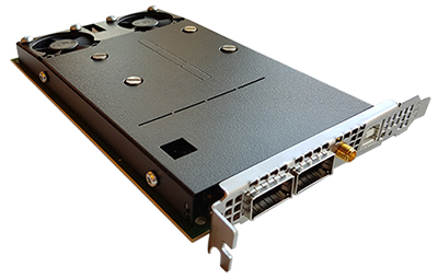
The standard configuration is based on the Xilinx Kintex UltraScale+ KU15P FPGA, to provide ample capacity for the dual QSFP28 interface.
The card features the KU15P to keep the solution as cost effective as high performance computing allows.
The card is mounted with 4 x 72-bit DDR4 ECC RAM, 4GB for a total of 16 GB.
檔案下載
-
- Xilinx® Kintex UltraScale+ XCKU15P FPGA
- 2 x QSFP28 ports
- 4 x 72-bit DDR4@2666MT/s (4 GB per bank with ECC)
- Support for direct Card to Card interconnect with up to 150Gbit/s
- Configuration flash RAM for boot images
- PCIe form-factor: Full height, half length (111.15 x 167.65 mm with bracket)
- On-board power and temperature sensors
- FPGA controlled link and status LEDs
- Active and passive cooling alternatives available
-
General Technical Specifications
Host Interface - Physical bus connector: 16-lane PCIe
- PCIe bus type: 1-16 lane PCIe Gen1/Gen2/Gen3
- Support for SMBUS
Network Interface - IEEE standard: IEEE 802.3 10/40/25/100 GE
- Physical interface: 2 x QSFP28 ports
- Supported QSFP+/QSFP28 modules: including fan-out modules for 4x10G/4x25GE, multimode SR4 (850nm), singlemode LR4 (1310nm), multimode LRM4 (1310 nm), or direct Attached Copper (Twinax) and others.
- Data rate: 8×10, 2×40, 8×25, 2×100 Gbps
- Support for SyncE
Configuration - Quad SPI fast parallel programming interface from supporting preprogrammed controller
- Configuration flash supports two boot images with automatic fallback to fail safe image if first image fails
- Upload of FPGA configuration to flash via PCIe or directly from Xilinx Vivado via the onboard JTAG dongle
- Direct FPGA configuration from Xilinx via the onboard JTAG dongle
- Support for encrypted FPGA bit file (optional)
- Supports Tandem PROM boot
On-Board Memory - 4 x 72-bit DDR4@2666MT/s (4 GB per bank with ECC)
- User configurable space in flash RAM for permanent storage
- Configuration flash RAM for boot images
On-Board Clock - PCIe clock: 100 MHz
- 2 x differential 161.13 MHz SerDes clock for Ethernet
- 2 x differential 161.13 MHz SerDes clock for Expansion
- 2 x differential 266.67 MHz clock for Memory
- 50 MHz clock
FPGA details FPGA Xilinx Kintex Ultrascale+ XCKU15P Environment - Physical dimensions: Full height, ½ length 111.15 x 167.65 mm with bracket
- Storage temperaure: -30 – 70°C , -22 – 158°F
- Operating temperature: 0 – 55°C, 30 – 130°F
- Operating humidity: 20 – 80%
- Hardware compliance: RoHS, CE
Additional Board Support - On-board power and temperature sensors
- FPGA controlled Link and Activity LED for each port. 4 for each QSFP.
- Board status LEDs
- Battery holder for coin cell battery for back-up of Key memory for bitstream encryption. (optional)
- Failsafe button on bracket
- PPS clock synchronization connector
- Support for direct Card to Card interconnect with up to 150Gbit/s
Power - Max 120W, above 75W PCIe AUX power must be used
- Active and passive cooling alternatives available
- Power, temperature and FAN tacho sensor reading
- PCIe AUX power connector available
On-Board Microcontroller - Board management Microcontroller for various internal control tasks as well as external communication
- SMbus/I2c
- Possible to readout telemetry parameters
-
P/N
Description
fb2CG@KU15P Xilinx® Kintex UltraScale+ XCKU15P FPGA
-
功能說明
- Xilinx® Kintex UltraScale+ XCKU15P FPGA
- 2 x QSFP28 ports
- 4 x 72-bit DDR4@2666MT/s (4 GB per bank with ECC)
- Support for direct Card to Card interconnect with up to 150Gbit/s
- Configuration flash RAM for boot images
- PCIe form-factor: Full height, half length (111.15 x 167.65 mm with bracket)
- On-board power and temperature sensors
- FPGA controlled link and status LEDs
- Active and passive cooling alternatives available
-
技術規格
General Technical Specifications
Host Interface - Physical bus connector: 16-lane PCIe
- PCIe bus type: 1-16 lane PCIe Gen1/Gen2/Gen3
- Support for SMBUS
Network Interface - IEEE standard: IEEE 802.3 10/40/25/100 GE
- Physical interface: 2 x QSFP28 ports
- Supported QSFP+/QSFP28 modules: including fan-out modules for 4x10G/4x25GE, multimode SR4 (850nm), singlemode LR4 (1310nm), multimode LRM4 (1310 nm), or direct Attached Copper (Twinax) and others.
- Data rate: 8×10, 2×40, 8×25, 2×100 Gbps
- Support for SyncE
Configuration - Quad SPI fast parallel programming interface from supporting preprogrammed controller
- Configuration flash supports two boot images with automatic fallback to fail safe image if first image fails
- Upload of FPGA configuration to flash via PCIe or directly from Xilinx Vivado via the onboard JTAG dongle
- Direct FPGA configuration from Xilinx via the onboard JTAG dongle
- Support for encrypted FPGA bit file (optional)
- Supports Tandem PROM boot
On-Board Memory - 4 x 72-bit DDR4@2666MT/s (4 GB per bank with ECC)
- User configurable space in flash RAM for permanent storage
- Configuration flash RAM for boot images
On-Board Clock - PCIe clock: 100 MHz
- 2 x differential 161.13 MHz SerDes clock for Ethernet
- 2 x differential 161.13 MHz SerDes clock for Expansion
- 2 x differential 266.67 MHz clock for Memory
- 50 MHz clock
FPGA details FPGA Xilinx Kintex Ultrascale+ XCKU15P Environment - Physical dimensions: Full height, ½ length 111.15 x 167.65 mm with bracket
- Storage temperaure: -30 – 70°C , -22 – 158°F
- Operating temperature: 0 – 55°C, 30 – 130°F
- Operating humidity: 20 – 80%
- Hardware compliance: RoHS, CE
Additional Board Support - On-board power and temperature sensors
- FPGA controlled Link and Activity LED for each port. 4 for each QSFP.
- Board status LEDs
- Battery holder for coin cell battery for back-up of Key memory for bitstream encryption. (optional)
- Failsafe button on bracket
- PPS clock synchronization connector
- Support for direct Card to Card interconnect with up to 150Gbit/s
Power - Max 120W, above 75W PCIe AUX power must be used
- Active and passive cooling alternatives available
- Power, temperature and FAN tacho sensor reading
- PCIe AUX power connector available
On-Board Microcontroller - Board management Microcontroller for various internal control tasks as well as external communication
- SMbus/I2c
- Possible to readout telemetry parameters
-
訂購資訊
P/N
Description
fb2CG@KU15P Xilinx® Kintex UltraScale+ XCKU15P FPGA